Chiplets are here, and more are coming. They can overcome the yield limitations of large ASICs, support a mix-and-match strategy for heterogeneous semiconductor IPs and multiple process nodes, improve thermal performance, and speed time to market. They are being used in a range of high-performance computing (HPC) applications, notably generative artificial intelligence (AI) and machine learning (ML) systems.
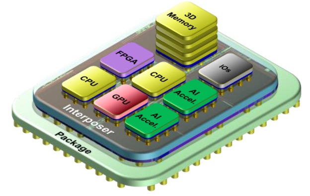
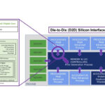
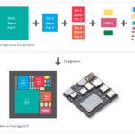
In contrast with a printed circuit board (PCB) based design that uses packaged ICs, chiplets use a bare die that is placed on a substrate or interposer that provides power and signal connections, usually to a PCB. Chiplets often include heterogeneous ICs from different vendors, using different process nodes and even different materials. They support high-speed connectivity and are delivered in a ball grid array (BGA) or land grid array (LGA) package (Figure 1).
Chiplets are integrated using three primary technologies, depending on the complexity of the design and cost and yield considerations:
- 2.5D, where devices are in the same plane on top of an interposer.
- 3D, where devices are stacked vertically on an interposer.
- Combined 2.5D and 3D, where some devices, like memory, are stacked vertically, and other devices are integrated on a single plane (see Figure 1).
The primary advantage of using chiplets in most systems is increased functional density. Other benefits of using chiplets include:
Increased yields from using smaller and simpler ICs. Large ICs like application-specific integrated circuits (ASICs) or field programmable gate arrays (FPGA) can experience yield challenges. Using multiple smaller dies increases overall yield. In addition, chiplets use a known good die that is tested prior to integration, further increasing yields.
Multiple process nodes and different materials can be integrated into a chiplet, with each process node and material used to provide an optimal mix of performance versus cost.
Chiplets support design reuse. Once designed, a chiplet can be reused in additional systems, and systems with chiplets can be designed to be modular and easily expandable. That can speed up time to market and reduce the cost of subsequent system development efforts.
Evolving and emerging chiplet interconnects
Chiplets are still primarily based on proprietary technologies, with each manufacturer using their own interconnect structure. But that’s beginning to change. For example, JEDEC has developed the high-bandwidth memory (HBM) standards for stacked DRAM. The Open Compute Project includes large users of chiplets and is developing their Open Domain-Specific Architecture (ODSA) initiative for chiplets.
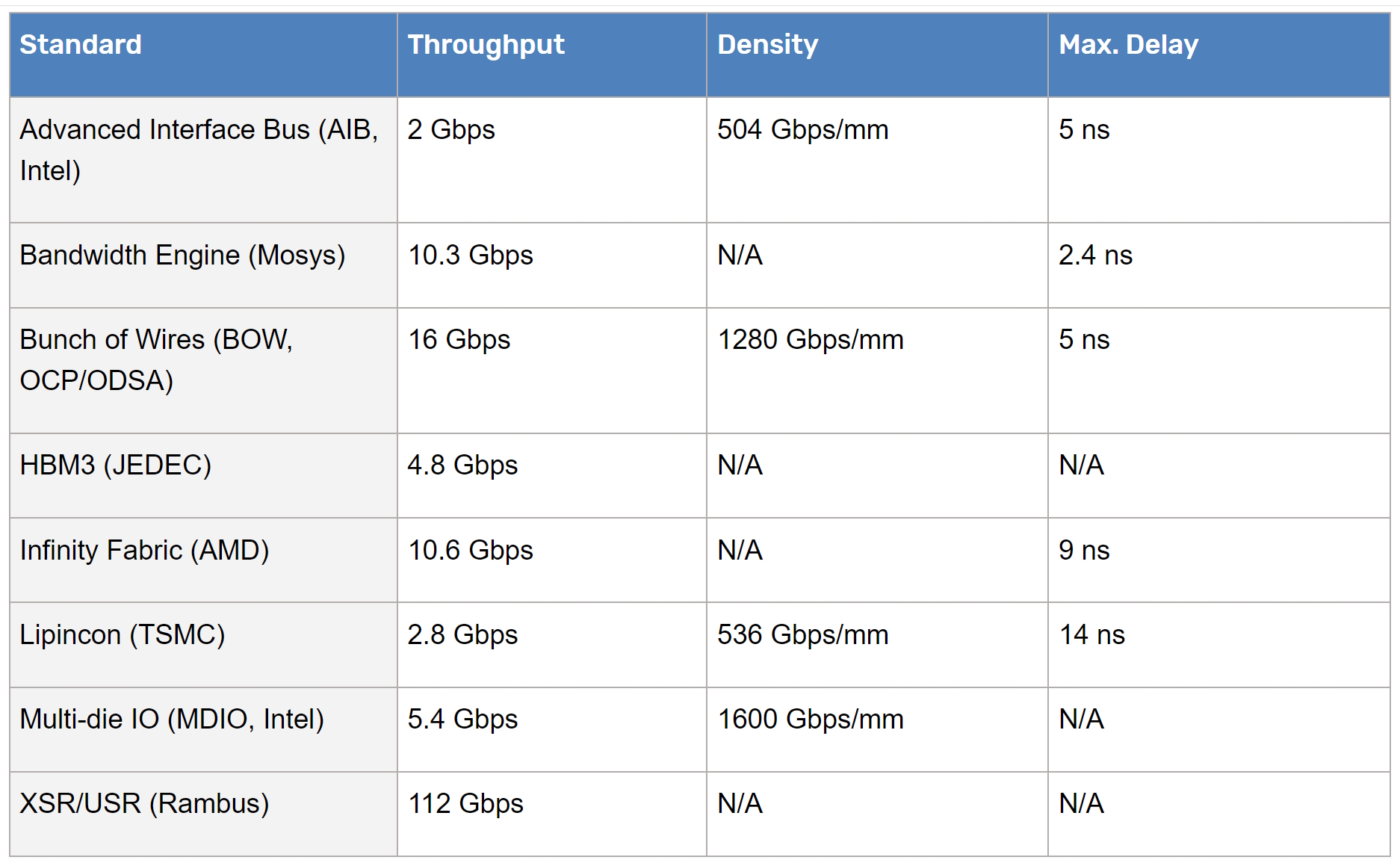
In addition, there are a bunch of wires (BoW) and Universal Chiplet Interconnect (UCIe) standards that support chiplet interoperability. The Open Compute Project has adopted boW for ODSA. UCIe is targeting the same applications as BoW but offers higher performance (Table 1).
Active interposers and optical I/Os
As in other areas of chiplet technology, interposers are evolving to deliver higher levels of performance. Passive interposers are fabricated from silicon, glass, and organic laminates. They serve the same purposes as a PCB and provide physical support for the chips, include interconnects, and enhance thermal management. However, the performance of passive I/Os, especially their limited bandwidth, can become a limitation for overall chiplet performance.
To provide increased I/O performance, two types of active interposers are emerging. The first active interposers include integrated active circuitry to support higher-performance interconnects. More recently, in-package optical I/O (IOI) has been introduced. Increasing the bandwidth of electrical active interposers is accompanied by higher power consumption and increased latency. It’s expected that the development of IOI technology will lead to increased performance for all key metrics, including reach, bandwidth density, power consumption, and latency.
Summary
Chiplets based on proprietary technologies are already here and are supporting generative AI and other HPC applications. There are currently several standardization activities underway to develop the open ecosystem needed to support the broader development of interoperable chiplets from different vendors.
References
96-Core Processor with 6 Chiplets 3D-Stacked on an Active Interposer with Distributed Interconnects and Integrated Power Management, IEEE Journal of Solid-State Circuits
An Overview of Chiplets for Systems Designers, Cadence
Challenges and Opportunities to Enable Large-Scale Computing via Heterogeneous Chiplets, arXiv
Overview of Active Interposers, Cadence
The Ultimate Guide to Chiplets, anysilicon
Unlocking on-device generative AI with an NPU and heterogeneous computing, Qualcomm
Leave a Reply