The packaging options for digital ICs (and the related buzz words and acronyms) continue to multiply. Advanced digital ICs such as microprocessors, field-programmable gate arrays (FPGAs), and application specific custom ICs (ASICs) are offered in a wide array of package styles such as: QFN, quad flat no leads; FBGA, fine pitch ball grid array; WLCSP, wafer level chip scale package; FOWLP, fan-out wafer-level package; fcCSP, flip-chip chip scale package; and FCBGA, flip chip ball grid array.
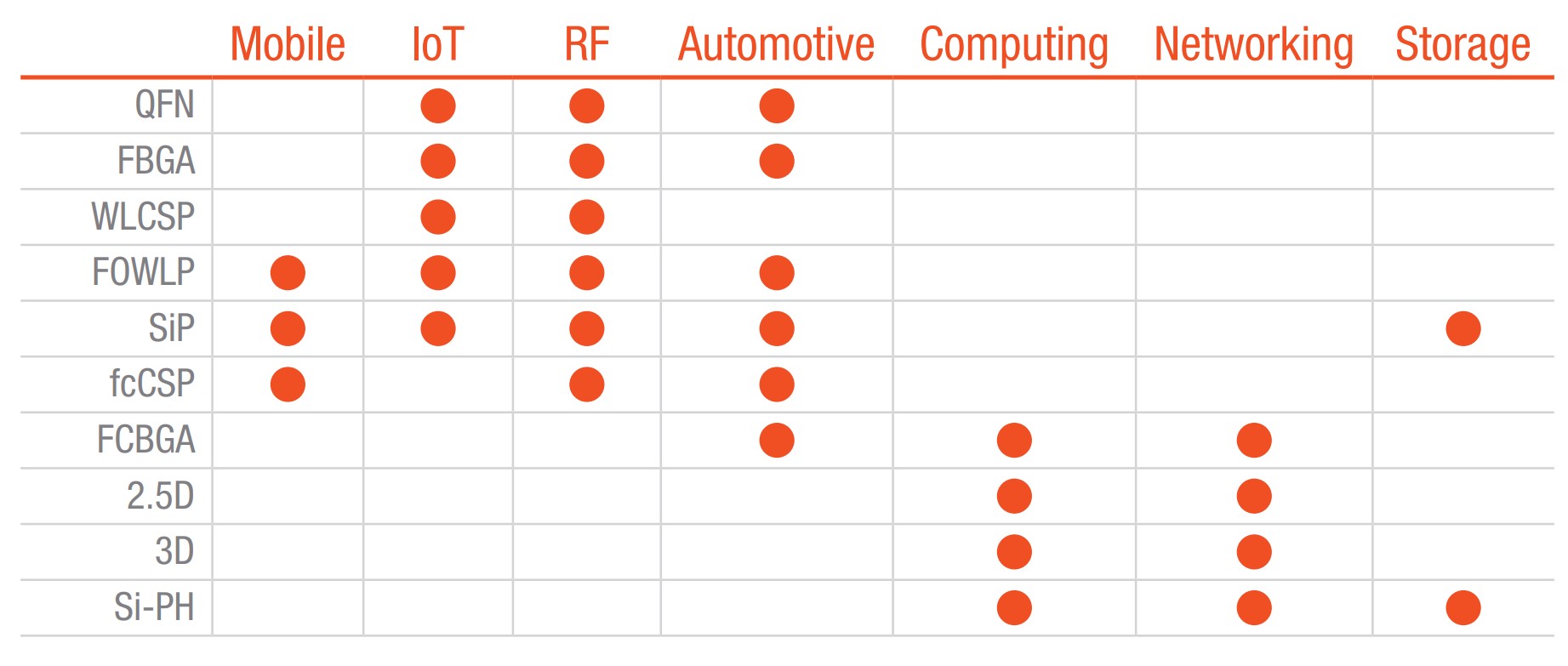
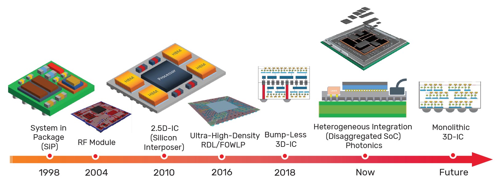
The options for packaging multiple chips together include system in package, multi-chip modules, chip-scale, chiplet, heterogeneous, 2.5D and 3D stacking, and more. Multi-chip quantum processors are being developed that can solve key scaling challenges toward a fault-tolerant quantum computer. And co-packaged optics (CPO), or in-package optics (IPO), are emerging that bring optics and switch silicon together in the same package creating a synergy between once disjoint and independent technologies and saving significant power.
Chiplets, MCMs and SiPs
Chiplet based designs, multi-chip modules (MCMs), and system in package (SiP) are or can be forms of heterogeneous integration, and there are very large grey areas when defining these three packaging styles. One company’s chiplet-based design may be called an MCM by another supplier, and MCMs and SiPs are often lumped into the same category. Some of the nuances are reviewed below.
A chiplet is a physical realization of a tested IP function with a standard communication interface manufactured on a silicon wafer to reduce cost by increasing the manufacturing yield and reusability across applications. Chiplets in a given solution can have different process nodes. Chiplets provide standard functions and enable designers to focus on the unique IP in their design. The result has been called a “pseudo-SoC” designed faster and at lower cost than a fully integrated SoC solution. Chiplet-based solutions generally do not include passive devices or other “non silicon” devices. An example of a chiplet solution can be some of today’s microprocessors where the processor core and I/Os reside on different silicon chips in a common package.
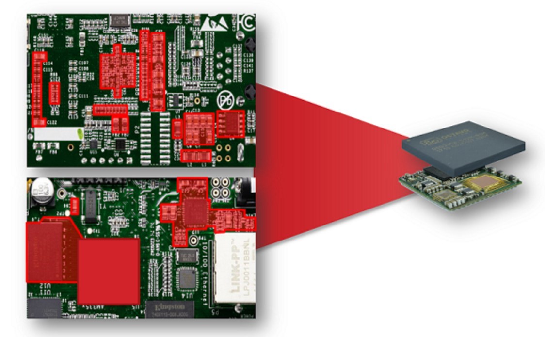
MCMs initially integrated only multiple chips and didn’t include passives or other components. And the chips in an MCM were “complete” ICs such as processors, GPU, and RF sections, not simpler single-function chiplets. As the concept evolved, MCMs grew in size and integrated additional components, and the SiP was born. The main difference between an MCM and a SiP is that an MCM does not have to be a complete system. By definition, a SiP is a system in a single package.
A MCM is a tightly coupled subsystem or module in a package. A SiP integrates multiple ICs along with supporting passive devices into a single package. Like MCMs, SiPs can use silicon from the best individual processes or process nodes to optimize performance and achieve the desired integration. A SiP is designed as a complete system and used as a single component.
2.5D and 3D packages
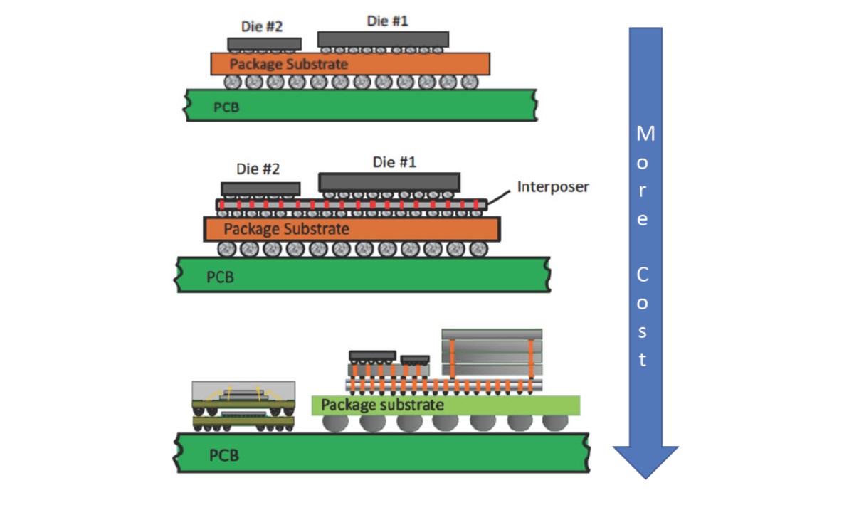
The use of through-silicon vias (TSVs) for interconnecting multiple dies is generally considered the difference between an MCM or SiP and a 2.5D packaged device. TSVs provide a high-density alternative to the organic substrates found in MCMs and SiPs. The use of TSVs gains some of the benefits of 3D packaging without the challenges and costs associated with fully 3D approaches. Placing several dies on an interposer with very fine pitched TSVs results, in short, interconnects and better weight, size, and power characteristics compared with a conventional MCM or SiP solution.
A fully 3D IC goes one step further and stacks in the vertical dimension using TSVs. It can result in smaller and higher-performance solutions. 3D packaging is another form of vertical integration that refers to 3D integration using interconnect methods such as wire bonding and flip chip. 3D packaging can be classified as 3D system in package (3D SiP), 3D wafer-level package (3D WLP), and 3D package on package (3D PoP). Compared with 2.5D packaging, the various forms of 3D packaging can have some drawbacks, including:
- Thermal performance can be improved by placing dies side by side instead of stacking them vertically.
- 3D structures are inherently more complex, and modifying or upgrading 2.5D assembly is usually simpler and faster. Upgrading a 2.5D device be as easy as using a new interposer or replacing one or more dies with improved versions.
.
Wafer-level and chip-scale
With wafer-level packaging (WLP), the wafer fabrication process is extended to include device interconnection before wafer dicing. Most other packaging do wafer dicing first, and then put the individual die in a plastic package and attach the solder bumps. WLP attaches the bottom, and top output layers of the package and the solder bumps to ICs before dicing the wafer. Since the package is essentially the same size as the die, WLP is a form of chip-scale package (CSP) technology.
WLP is used in applications that demand the smallest possible solution, such as smartphones. However, the limitation of WLP is the limited number of contacts that can be supported as a result of the very small package size. In highly complex and compact systems, fan-out wafer-level packaging (FO-WLP) enhances standard WLP to overcome the limited I/O capabilities.
FO-WLP enables a smaller package footprint along with improved thermal and electrical performance compared to conventional packages. Still, FO-WLP is larger than WLP, and FO-WLP supports a higher number of contacts without increasing the die size. In FO-WLP, the wafer is diced first, then the dies are repositioned precisely on a carrier wafer, with an area for fan-out around each die. The dies are molded, and then the solder balls are added.
Co-packaged optics
The serialization-deserialization (SerDes) function in high-speed digital networks, such as hyperscale data centers, typically involves an interface between silicon-based communication links and optical-based links. As the distance between the optical engine and the switch silicon decreases, the channel insertion losses also drop, saving significant power. The closest spacing is achieved with co-packaged optics (CPO), where both sides of the interface are in a single package.
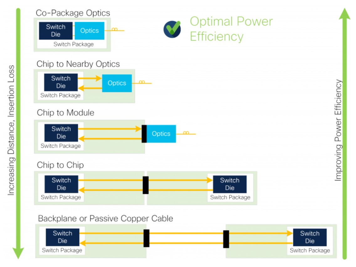
Two of the efforts underway to develop CPO are the Consortium for On-Board Optics (COBO) and the Co-Packaged Optics Joint Development Foundation (CPO JDF). COBO has created a CPO Working Group focused on developing technical guidance and standards for CPO implementations. It is made up of end users and technology suppliers interested in the use of CPO in hyperscale data centers. The COBO activities are primarily interested in the remote laser sources and optical connectivity required for CPO implementations, and it is expected to be complementary to other CPO standardization activities.
Facebook and Microsoft established the CPO JDF, and its primary considerations are related to the system integration concerns related to CPO. A product requirements document (PRD) has been released by the CPO JDF describing an 8x400G CPO module targeted to increase network switch density and increase power efficiency. The PRD calls for the use of the XSR (extremely short reach) interface. XSR is optimized for die-to-optical engine (D2OE) interfaces and die-to-die (D2D) interfaces across package substrates up to about 100 mm × 100 mm.
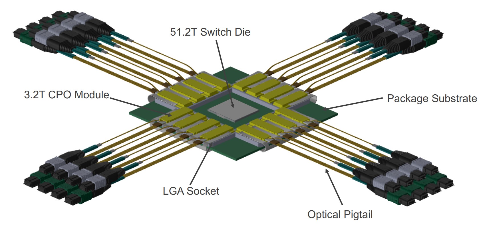
Sixteen of the XSR CPO modules will be used to build a low-power 51.2Tb/s switch. The PRD defines two variations of the CPO modules, one supporting 400GBASE-FR4 (8 Tx/Rx fiber pairs) and one supporting 400GBASE-DR4 (with a total of 32 Tx/Rx fiber pairs).
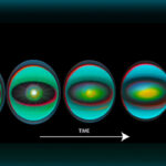
Multi-chip quantum processors
Scaling quantum computers is challenging. As the quantum processors grow in size, manufacturing yields decline. Large numbers of quantum bits (qubits) are needed to implement error-corrected quantum computing. Efforts are underway to connect multiple smaller dies into a large-scale quantum processor. This multi-chip approach is expected to simplify the creation of large quantum processors and support predictable and accelerated scaling of the technology.
Scaling is key to the development of fault-tolerant quantum computers. An 80-qubit system is expected to be tested later this year. Applying multi-chip module technology to quantum processors could lead to large enough systems to run practical applications, including the needed error correction.
Summary
There’s a growing multiplicity of packaging choices for digital ICs, optical interconnects, and quantum processors. Advanced packaging technologies support heterogeneous integration and the use of ICs from the best individual processes or process nodes to optimize performance and achieve the desired integration. Continued packaging developments will be important to enable advanced system solutions from mobile phone handsets to hyperscale datacenters.
References
2.5D/3D Packaging, NASA
Chiplets and Heterogeneous Packaging Are Changing System Design and Analysis, Cadence Design Systems
Consortium for On-Board Optics
Co-Packaged Optics and an Open Ecosystem, Cisco Systems
Co-Packaged Optics Collaboration Joint Development Forum
Recent Advances in Thermal Metamaterials and Their Future Applications for Electronics Packaging, ASME
Rigetti Computing introduces world’s first scalable multi-chip quantum processor, Rigetti Computing
SiP Technology, Octavo Systems


Leave a Reply